Adisyn may have a fix for the Chip Industry’s Wiring Problem
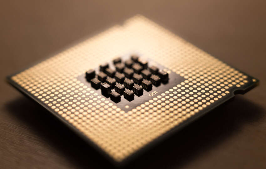
Think about the wiring inside a computer as an incredibly small highway system, with billions of lanes carrying electrical signals between transistors, the tiny switches that flip between 0 and 1. Today, that wiring is mostly made from copper, which has made sense for years because copper is highly conductive.
The issue is that chips are getting smaller, denser, and more powerful, and copper is starting to hit its limits. It generates too much heat, uses more power, and becomes less efficient as everything is pushed to smaller scales.
That is why graphene has long been viewed as such an attractive replacement. It is only one atom thick, conducts electricity better, runs cooler, and does not suffer the same performance drop-off as copper at very small dimensions. The challenge has never really been the theory. It has been whether graphene could actually be grown in a way that works inside a real chip factory.
That is what Adisyn (ASX:AI1) has now demonstrated through its subsidiary 2D Generation. The company has integrated a graphene layer onto a small copper surface using the same manufacturing equipment already used in chip fabrication, and at temperatures low enough not to damage the chip.
Why the Temperature Limit Matters So Much
In semiconductor fabrication, chips are built in many layers, and once those layers are in place you cannot simply come back later and apply a process at much higher temperatures. If you do, you risk damaging the structure that has already been built and compromising the whole chip.
That is why temperature matters so much. The practical threshold is around 450°C. Go above that and the risk of damaging the chip rises quickly.
What makes Adisyn’s result important is that it developed a way to add this new material below 450°C. That means the process has a far better chance of fitting into a real semiconductor manufacturing flow rather than just working in a lab.
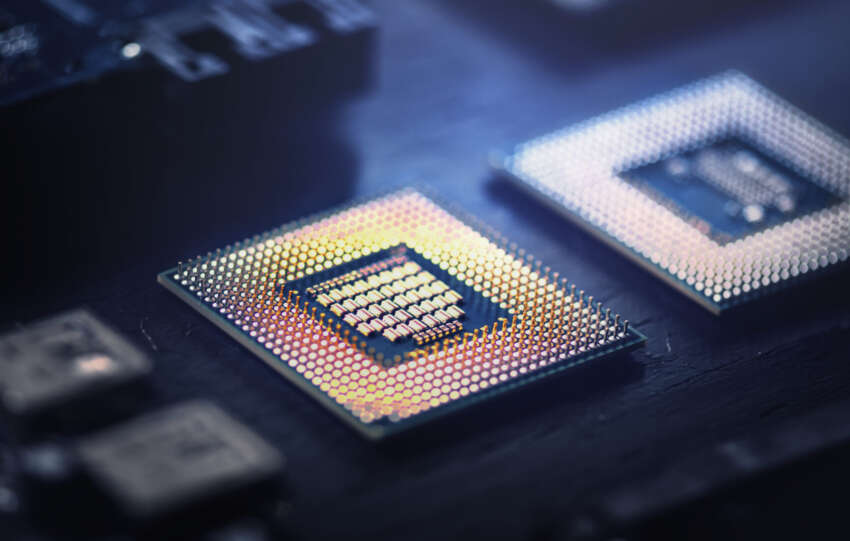
A $1 Trillion Industry With a Wiring Problem
As chips keep shrinking, with the industry now moving below 2nm and TSMC already pushing beyond that, copper wiring is becoming so thin that it starts to behave unpredictably. At that scale, electrical signals are disrupted more easily, resistance rises, and energy use increases.
That is the heart of the interconnect problem. It is now one of the main constraints on how much further AI chips, GPUs, and smartphones can keep advancing.
The opportunity is large. The company estimates the addressable market could be worth more than A$1 trillion by the early 2030s. If graphene interconnects are adopted at scale, each chip using the technology could create royalty or licensing revenue because Adisyn owns the IP.
That is what makes the model interesting. This is not just about supplying a material. It points to a potential IP licensing business, where the upside comes from adoption across the industry rather than trying to manufacture every part itself.
What the Tests Actually Proved
For investors looking at what Adisyn has achieved so far, the company has demonstrated an unbroken graphene layer on chips that is just 1nm thick on a copper surface.
Just as importantly, the process was run below 450°C and used industrial-grade manufacturing equipment that is already familiar to the semiconductor industry. That is a big part of why the result stands out. It suggests the technology may have a realistic path into existing chip fabrication processes.
The next key focus is scaling. The company now needs to move from this proof point to wafer-level testing, initially at the 300mm wafer scale, and then prove repeatability and consistency.
That is the real test from here. Early technical success matters, but investors will want to see whether the process can be repeated reliably and scaled in a way that chipmakers could actually use.
The overlooked upside for AI1: Graphene drone coatings to make them stealthier
AI1 is now targeting global tier 1 semiconductor players such as TSMC, Samsung, and Intel, the foundries and chipmakers that actually manufacture advanced semiconductors at scale. These discussions are still likely to be early, but the company is now taking the right steps to be in those conversations.
That matters because technical proof alone is not enough. The real commercial value only starts to open up once the major industry players are willing to engage.
There is also a second opportunity sitting underneath the main semiconductor story, and that is the defence and UAV angle. Adisyn is developing graphene-based composite materials designed to reduce radar signatures in UAVs and other defence platforms.
In simple terms, that means making drones and aircraft harder to detect. It could become a very valuable parallel track for the business.
The company has not gone into much detail on that side in this announcement, so it remains more of a watch point than a near-term driver. Still, it is one worth keeping an eye on in future updates, because this is a massive growth market for Adisyn in addition to the semiconductor equipment market.
Pitt Street Research Directors owns shares in the company discussed. This article reflects personal views and is not financial advice.