Investment Case Summary
- Tape-out moves the RRAM program from design theory into physical silicon at a TSMC-compatible flow.
- Wafer-level electrical test data, not tape-out itself, is the real gating event for the thesis.
- Compute-in-Memory validation is what connects the chip back to exoskeleton and robotics revenue paths.
Silicon now goes into fabrication with TSMC wafers, and the next 12 months become an execution test
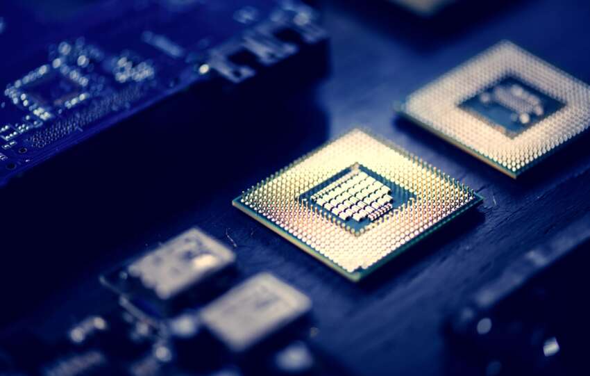
dorsaVi (ASX:DVL) has commenced tape-out of its first RRAM-CMOS validation chip, the step that pushes the program out of the design suite and into a semiconductor fab. For a micro-cap that has spent almost two years asking investors to believe in a roadmap, this is the moment the roadmap starts becoming silicon.
The chip uses commercial CMOS front-end wafers sourced through TSMC, with partner-led back-end-of-line steps stacking the RRAM layer on top. RRAM is resistive random-access memory, a fast, low-power, non-volatile chip technology being pitched as the memory layer for edge AI. In plain English, dorsaVi is bolting its memory onto a standard foundry process rather than trying to build a bespoke platform.
That is the part of the announcement most investors will skim past. It is also the part that quietly determines whether this ever gets to commercial scale.
We think today’s announcement is best read as a sequel to January’s design finalisation. The design was the theoretical proof. The tape-out is the practical one. Everything from here is about whether the silicon behaves the way the design says it should.
Why tape-out changes how investors should weight this program
Until today, the RRAM story lived in simulations, projected performance metrics and a licence portfolio built with NTU Singapore and ITRI Taiwan. Tape-out is the point where those assumptions get tested against physical resistance states, sensing margins and process variation.
The validation chip is designed to generate electrical and process data on three things that matter. Memory array behaviour, write-and-verify circuitry, and Compute-in-Memory functionality. Each one has to work under real silicon conditions before dorsaVi can credibly pitch this to a foundry or fabless partner.
The skeptical read is that tape-out is not fabrication. Wafers still have to be run, BEOL integration has to hold, and wafer-level electrical testing has to return data that matches the design intent. The constructive read is that dorsaVi has now committed capital and calendar time to a real silicon program, which is a different kind of commitment than another press release about a licence.
The TSMC pathway keeps the manufacturing story credible
The staged silicon implementation uses commercial CMOS wafers from TSMC before partner-led BEOL integration stacks the RRAM layer on top. That approach preserves two things. Foundry compatibility, and the option to migrate to a 22-nanometre node later without redesigning the transistor platform.
For a company of dorsaVi’s size, that discipline matters more than the chip itself. Micro-caps that ask foundries for bespoke work rarely reach production. Micro-caps that adapt to standard foundry flows sometimes do.
Our concern is that the partner-led BEOL step is still the weakest link in the manufacturability story. It has to work at wafer scale, not just on a validation die. Investors should treat the electrical test data expected from this program as the real gating event, not the tape-out itself.
Compute-in-Memory is what makes the market opportunity worth the risk
The validation chip embeds Compute-in-Memory macros directly into the RRAM array, so the same physical layer that stores data can also run calculations locally. In edge devices operating under tight power and latency budgets, that removes the biggest bottleneck in conventional architectures.
For dorsaVi, this is what connects the memory work back to the existing sensor business and to the exoskeleton and robotics use cases we covered earlier this year. If the chip does what the design says, the sensor stops streaming raw data and starts making decisions on the device itself.
That is the layer of the story global AI memory demand actually rewards. Local, low-power, non-volatile compute for robotics, EVs, defence and wearables. The commercial pitch only survives if the silicon proves the concept.
The Investors Takeaway for dorsaVi
Tape-out is the milestone dorsaVi’s equity story needed. It is also the point where the market can no longer credit the company purely on roadmap. From here, investors should be tracking wafer-level electrical test results, resistance-state separation data, and any early indication of interest from foundries or fabless customers.
We think the honest framing is that today’s announcement removes one execution risk and sharpens another. The design has been committed to silicon. Now the silicon has to deliver. Readers can see our prior coverage of the design finalisation at stocksdownunder, which sets out why the TSMC-compatible pathway matters for a company this size.
The stock will trade on the next data drop, not this one.
Pitt Street Research Directors owns shares in the company discussed. This article reflects personal views and is not financial advice.