Dorsavi’s ReRAM Strategy Leverages Specialists Across Design and Manufacturing
Dorsavi (ASX:DVL) has announced a collaboration with Nanyang Technological University (NTU), as it moves into the next phase of its 22nm ReRAM fabrication and co design program. This matters because NTU is the institute Dorsavi originally acquired the ReRAM IP from, and the company is also working alongside the Taiwan Industrial Technology Research Institute (ITRI) to support development.
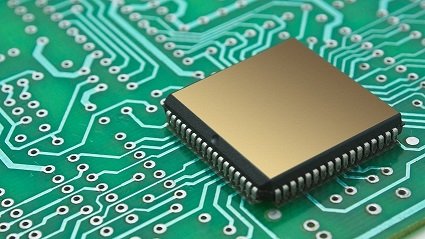
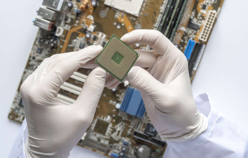
The goal here is that Dorsavi wants to advance its proprietary ReRAM platform from a 40nm node down to a 22nm node that is compatible with a commercial foundry CMOS process, which is essentially the standard manufacturing process used to produce modern chips at scale.
How the Partnership Works Dorsavi, NTU, and ITRI Split the Build
To help investors understand how this collaboration is expected to work, it can be viewed as a split of responsibilities across three specialist groups.
Dorsavi will define what the chip needs to do, where it will be used, and how the broader system should function in real world applications.
NTU will focus on the ReRAM architecture itself, designing the memory cells and engineering the structure of the memory stack.
ITRI’s role is then to translate that research level design into something that a chip manufacturer can actually build, by adapting it into a foundry ready process and manufacturing flow.
Overall, this structure is important because it combines different skill sets that are difficult for one organisation to hold internally. For investors, it signals that Dorsavi is leaning on credible technical partners to progress the milestone path toward a manufacturable ReRAM chip.
What are the Best ASX Stocks to invest in right now?

ReRAM Explained Why Multi Level Memory and 22nm Scaling Matter
Resistive RAM, or ReRAM, stores data by switching a memory cell between different resistance states.
Traditional memory is mostly binary, meaning each cell is either a 0 or a 1. ReRAM is different because the cell is not limited to just two states. It can be programmed to multiple stable resistance levels. A simple way to picture it is a dimmer switch instead of a light switch. You are not just turning something on or off, you can set it to different levels depending on what you need.
That matters because those “in between” levels can represent more information than a basic 0 or 1. It is also the foundation for compute in memory style processing, where parts of the calculation can happen inside the memory array itself, rather than constantly moving data back and forth between memory and a separate processor. Less movement usually means lower power use and faster response, which is especially important for devices doing work locally at the edge rather than relying on the cloud.
On the chip roadmap, the shift from 40nm to 22nm is essentially about shrinking the features on the chip so more can fit into the same area. In practical terms, that can enable:
Higher memory density per unit area, meaning more bits per mm²
Tighter integration between memory, compute blocks, and sensor interfaces
Lower energy per operation, because distances are shorter and the supporting circuitry can be more efficient
Putting it together, the move to 22nm is aimed at increasing memory and computational capacity while staying energy efficient, which is exactly the combination you want if the end goal is always on sensing, edge intelligence, and neuromorphic style workloads.
If you want to look into this more, we have a research note detailing this here.
Watch our interview with Group CEO Mathew Regan about the NTU collaboration!
What’s the Market for this Technology?
These chip designs have a clear fit in markets where devices need to sense, decide, and respond locally, with low power and low latency. That is especially relevant for robotics, where the closer you get to brain like processing at the edge, the more useful the hardware becomes.
Here is the big picture on where the demand pools sit today, based on third party market estimates:
- Robotics (primary): projected to reach US$372.59 billion by 2034
- Wearables: projected to reach US$186.14 billion by 2030
- Electric vehicles: projected to reach US$6.52397 trillion by 2030
- Industrial automation and control: projected to reach US$378.57 billion by 2030
- Neuromorphic computing: projected to reach US$20.27 billion by 2030
- Smart energy: projected to reach US$337.19 billion by 2030
- Edge AI: projected to reach US$66.47 billion by 2030
The key point for investors is not that DorsaVi or any single chip program captures a meaningful percentage of these headline markets. Most of that spend is not semiconductors, and the chip content inside each end product is only a slice of the total value.
But these figures do highlight the scale of the ecosystems these chips can plug into. The most relevant overlap is where always on sensing and local decision making matter, particularly robotics, industrial automation, wearables, and edge AI. Neuromorphic computing is smaller in dollar terms, but it is directly aligned with the compute in memory value proposition, which is why it is often the most strategically important segment to watch, and it’s also very early in its tech lifecycle.
The Investor’s Takeaway For DVL
The main takeaway for investors is that this technology is still early stage. More companies are starting to see the value of putting more “brain like” processing on the chip, but it is not yet proven at scale across mainstream products.
There are also real execution risks. The biggest technical hurdle is integrating the ReRAM layer into a foundry compatible back end manufacturing flow without hurting yield or long term reliability. On top of that, compute in memory and neuromorphic approaches are still not mainstream in many product categories, and chip design cycles are long. Progress tends to come in milestones, not in a smooth straight line.
The upside is that DorsaVi’s approach is designed to reduce those risks. Working with ITRI and anchoring the program on a commercial 22nm CMOS foundation is aimed at making the technology manufacturable, not just viable in a lab.
What we would watch next from DorsaVi is a small set of clear proof points:
- A 22nm integrated test vehicle: evidence the ReRAM can be built into a real chip process, even before full scale memory blocks are completed.
- Proof of multi-state compute in memory: demonstration that the memory can reliably hold multiple resistance levels and perform the intended compute in memory functions.
- Signs of foundry readiness: any mention of process design kit access, foundry enablement steps, or a lead customer moving into evaluation.
If these show up, they would be strong signals that the program is moving from research into a path that could support real products and eventual revenue.
Pitt Street Research Directors owns shares in the company discussed. This article reflects personal views and is not financial advice.